
Google’s Tensor G5: A Bold Leap Towards Independence with TSMC and Custom Innovations
Google’s foray into the world of custom silicon, marked by the introduction of the Tensor chip with the Pixel 6, has been a fascinating journey. Leveraging Samsung’s foundry and components, the initial Tensor chips provided Google with the means to tailor hardware to its specific software needs, particularly in the realm of AI and computational photography. However, the upcoming Tensor G5 promises a significant shift in strategy, signaling a move towards greater independence and a renewed focus on custom-designed components. This transition involves a switch to TSMC (Taiwan Semiconductor Manufacturing Company) for manufacturing, a strategic decision that necessitates a re-evaluation of the chip’s internal architecture and the sourcing of key components.
The core message is clear: Tensor G5, destined for the Pixel 10, will represent a departure from the heavy reliance on Samsung. While previous Tensor iterations were a blend of Google’s in-house designs and readily available Samsung components, the G5 is poised to incorporate a selection of "off-the-shelf" parts to fill the void left by Samsung’s departure. This isn’t necessarily a step back; rather, it’s a pragmatic approach to ensuring a smooth transition to a new manufacturing partner while retaining control over the most critical aspects of the chip.
Android Authority’s recent report sheds light on the specific components that are undergoing this transformation. Crucially, Google will retain and upgrade several of its proprietary designs that were integral to the success of previous Tensor chips. The Tensor Processing Unit (TPU), a dedicated accelerator for machine learning tasks, will undoubtedly continue to be a cornerstone of the Tensor architecture, enabling features like on-device AI processing and enhanced computational photography capabilities. Similarly, the Digital Signal Processor (DSP), responsible for handling audio and signal processing tasks, will likely remain a Google-designed component, ensuring optimized performance for audio recording, playback, and noise cancellation. The memory compressor, which optimizes memory usage to improve performance and power efficiency, and the audio processor, responsible for the intricacies of sound management within the device, will also likely persist as Google-designed elements. These components are deeply intertwined with Google’s software ecosystem and provide a unique advantage over relying solely on commercially available solutions.
The report highlights several key component swaps to accommodate the shift to TSMC. These swaps represent a careful balancing act between leveraging existing technology and forging new paths towards enhanced performance and control. While the specific manufacturers of these "off-the-shelf" components remain undisclosed, the selection process will undoubtedly be rigorous, ensuring compatibility, performance, and long-term reliability.
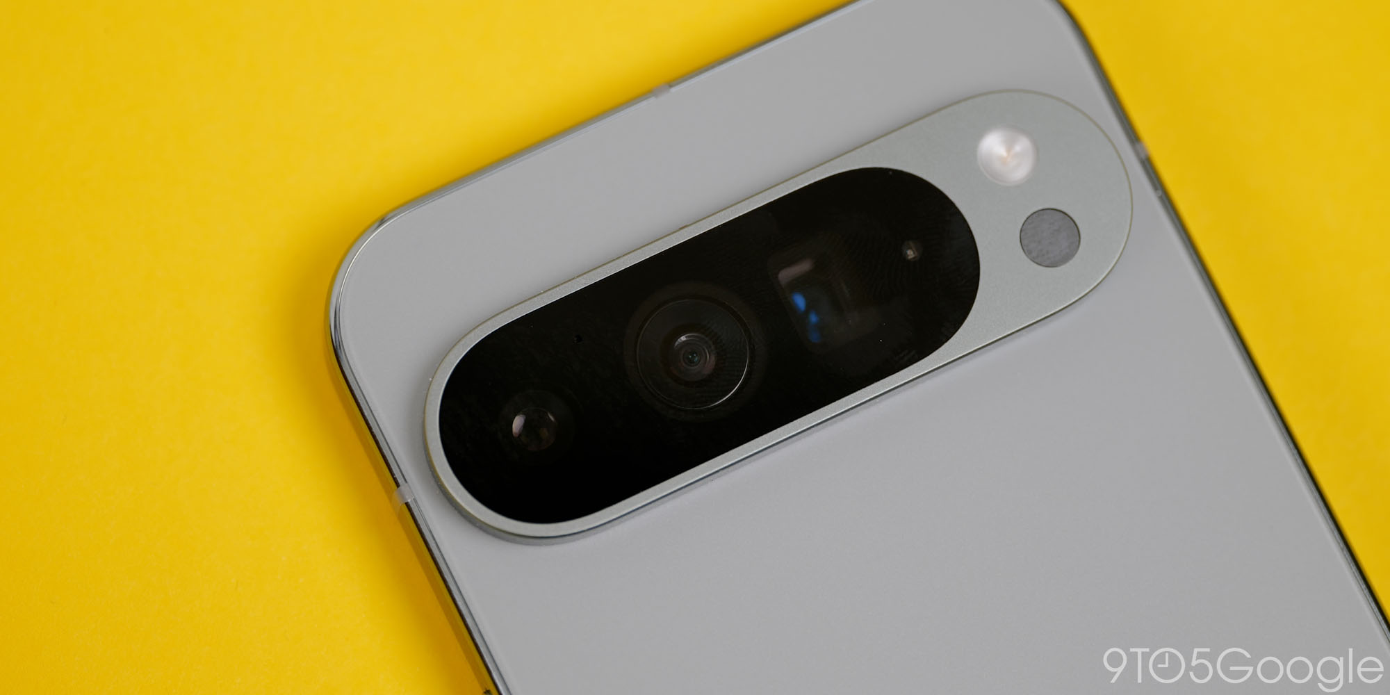
Perhaps the most significant change highlighted in the report is the introduction of a fully custom Image Signal Processor (ISP). The ISP is a critical component responsible for processing raw image data captured by the camera sensor and transforming it into the final image that users see. Google’s decision to develop a custom ISP signals a renewed focus on computational photography and a desire to further differentiate its Pixel phones through superior image quality.
This isn’t the first time Google has ventured into the realm of custom ISPs. The company previously experimented with dedicated image processing chips in its Snapdragon-powered Pixel phones, starting with the "Pixel Visual Core" in the Pixel 2 series in 2017. This chip significantly improved the speed and quality of HDR+ processing, a signature feature of Google’s camera software. The "Pixel Visual Core" evolved into the "Pixel Neural Core" with the Pixel 4, further expanding its capabilities to include on-device machine learning for image processing. However, Google abandoned this approach with the introduction of the Tensor chip in 2021, opting to integrate ISP functionality within the Tensor SoC.
The decision to resurrect a fully custom ISP for the Tensor G5 suggests that Google believes it can achieve even greater image quality and performance by decoupling the ISP from the main processor. This allows for a more specialized and optimized design, tailored specifically to the needs of Google’s camera algorithms. A custom ISP provides Google with greater control over the image processing pipeline, enabling them to implement cutting-edge features and algorithms that are not possible with commercially available solutions. This could translate into improvements in areas such as dynamic range, low-light performance, noise reduction, and computational photography features like Super Res Zoom and Magic Eraser.
Beyond the ISP, another notable component swap involves the modem. It has been previously reported that Google will be using a MediaTek modem in place of the Samsung modems used in previous Tensor chips. This is a significant shift, as the modem is responsible for cellular connectivity, including 5G, 4G LTE, and older network technologies. MediaTek has emerged as a major player in the modem market, offering competitive performance and features. This move may be driven by a combination of factors, including cost considerations, performance requirements, and strategic partnerships. The MediaTek modem will need to be tightly integrated with the Tensor G5 to ensure seamless connectivity and optimal performance.
The transition to TSMC and the incorporation of "off-the-shelf" components, including the custom ISP and the MediaTek modem, represent a significant undertaking for Google. While the company will retain and upgrade its own designs for key components like the TPU, DSP, memory compressor, and audio processor, the changes implemented to accommodate the new manufacturing process will undoubtedly have an impact on the overall performance and capabilities of the Tensor G5.
The ultimate question is whether these changes will be noticeable to the end user. In many ways, Google is striving to maintain the same level of performance and functionality that users have come to expect from its Pixel phones. However, the new architecture and components could potentially lead to improvements in certain areas, such as image quality, power efficiency, or cellular connectivity. Conversely, there is also the potential for unforeseen downsides, although Google will undoubtedly be working diligently to mitigate any risks.
The Tensor G5 represents a bold step towards greater independence for Google in the realm of custom silicon. By switching to TSMC and incorporating a mix of custom-designed and "off-the-shelf" components, Google is taking greater control over its hardware destiny and paving the way for future innovations in its Pixel phones. The introduction of a fully custom ISP is particularly exciting, as it suggests a renewed focus on computational photography and a desire to push the boundaries of what’s possible with smartphone cameras. The Pixel 10, powered by the Tensor G5, will be a fascinating showcase of Google’s hardware and software expertise. The world eagerly awaits the results of this ambitious endeavor.